IRTUM – Institutional Repository of the Technical University of Moldova
TEM investigation on new microstructures and properties of GaN
- Home
- →
- Facultatea Calculatoare, Informatică şi Microelectronică
- →
- Prezentări
- →
- View Item
JavaScript is disabled for your browser. Some features of this site may not work without it.
| dc.contributor.author | SCHÜRMANN, U. | |
| dc.contributor.author | WOLFF, N. | |
| dc.contributor.author | CIOBANU, V. | |
| dc.contributor.author | DENG, M. | |
| dc.contributor.author | KAMP, M. | |
| dc.contributor.author | RAEVSCHI, S. | |
| dc.contributor.author | BRANISTE, T. | |
| dc.contributor.author | SCHÜTT, F. | |
| dc.contributor.author | ADELUNG, R. | |
| dc.contributor.author | TIGINYANU, I. | |
| dc.contributor.author | KIENLE, L. | |
| dc.date.accessioned | 2022-05-12T07:16:32Z | |
| dc.date.available | 2022-05-12T07:16:32Z | |
| dc.date.issued | 2018 | |
| dc.identifier.citation | SCHÜRMANN, U., WOLFF, N., CIOBANU, V. et al. TEM investigation on new microstructures and properties of GaN [Resursă electronică]: prezentare în cadrul conf. intern. “The 19th International Microscopy Congress (IMC19)”, 9-14 Sept. 2018, Sydney, Australia. | en_US |
| dc.identifier.uri | https://tinyurl.com/23v8hb2m | |
| dc.identifier.uri | http://repository.utm.md/handle/5014/20263 | |
| dc.description | Acces full text - https://tinyurl.com/23v8hb2m | en_US |
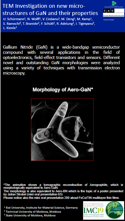
| dc.description.abstract | Gallium Nitride (GaN) is a wide-bandgap semiconductor compound with several applications in the field of optoelectronics, field-effect transistors and sensors. Different novel and outstanding GaN morphologies were analyzed using a variety of techniques with transmission electron microscopy. Wurtzite-phase bulk GaN single crystals with the thickness of 300 µm were grown by hydride vapor phase epitaxy (HVPE). The single crystals proved to exhibit fine modulation of doping related to the spatial distribution of impurities. Self-organized three-dimensional architectures were brought to light by using photoelectrochemical etching techniques which are highly sensitive to local doping. Electron diffraction pattern show an unusual departure of a few degrees from orthogonal wurtzite structure angles. These deviations are probably strain-induced. Extremely porous, mechanically flexible and stretchable aero-GaN was fabricated using flame made tetrapodal ZnO as sacrificial templates. GaN layer grown by HVPE in combination with template removal made it possible to fabricate hollow GaN microstructures with traces on the inner surface of crystalline ZnO with outstanding chemical stability. Besides, by using ZnO templates with additional deposited Au droplets on the surface for aero-GaN growth whiskers with crystalline droplets on top grow from the inside surface of the hollow structures. These structures could be interesting for biosensor applications. Furthermore one can exploit the plasmon excitation of the Au nanoparticles for optical applications. GaN samples were analyzed with different techniques inside a FEI Tecnai F30 STwin (300 kV). The crystalline structure was evaluated via high resolution TEM (HRTEM) and electron diffraction, while the chemical composition was analyzed with energy-dispersive X-ray (EDX) elemental mapping as well as energy filtered TEM (EFTEM). Additionally, the morphology was investigated with high annular dark field-scanning TEM (HAADF-STEM) and - in the case of gold structures inside the hollow aero-GaN tubes - STEM tomography. | en_US |
| dc.language.iso | en | en_US |
| dc.publisher | Australian Microscopy & Microanalysis Society | en_US |
| dc.rights | Attribution-NonCommercial-NoDerivs 3.0 United States | * |
| dc.rights.uri | http://creativecommons.org/licenses/by-nc-nd/3.0/us/ | * |
| dc.subject | single crystals | en_US |
| dc.subject | semiconductor compounds | en_US |
| dc.subject | transmission electron microscopy | en_US |
| dc.title | TEM investigation on new microstructures and properties of GaN | en_US |
| dc.type | Presentation | en_US |
Files in this item
The following license files are associated with this item:
This item appears in the following Collection(s)
 Except where otherwise noted, this item's license is described as Attribution-NonCommercial-NoDerivs 3.0 United States